|
|
|
|
|
|
|
|
||

|
|
||

|
|
||
|
|
|
||

|
|
||
|
|
|
||

|
|
||
|
|
|||

|
|
||

|
|
||

|
|
||
|
|

|
|
|
|
|
|
||
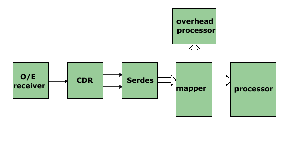
The high speed interface between the optical receiver and down stream hardware requires careful attention to detail. Sub-optimal design of this interface could, at best cause increased BER, and at worst, the complete interruption of traffic. High speed design skills are critical to allow optimum performance of the system at SONET speeds. Typically these designs involve a serial link from the receiver to a clock recovery device and deserialization to a more manageable bus speed. Once deserialized the data stream must be carefully routed to avoid timing skew between data bits. Traditional SONET designs use a mapper device to handle the overhead information and IP packet or ATM cell mapping in the SONET bit stream. This mapper may be implemented in a programmable FPGA device, bought as a chip, or designed as part of an ASIC. The mapper output could be passed to an embedded controller for further processing or through a switch fabric to implement a SONET switch.

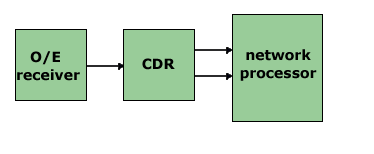
The trend with newer designs is greater integration of the various building blocks. Using a high speed network processor allows real time processing of the SONET data as it flows through the processor. Some of these processors also incorporate the SONET mapper function which removes the need for an external device.
